Magic is an interactive system for creating and modifying VLSI circuit
layouts. With
Magic, you use a color graphics display and a mouse to design basic cells
and
to combine them hierarchically into larger structures. Magic has built-in
knowledge of layout rules - as you are editing, it continuously checks for
rule violations. It has a built-in circuit extractor: from the layout, the
extractor creates an output file suitable for use with circuit simulation
tools such as Spice (for detailed, mixed-signal simulation) or IRSIM (for
digital simulation).
Magic must be run from a workstation
that supports the Unix X
Windows system (although it can be easily compiled for Linux at home.
Please contact me if you need help in
doing this). Once you login to the Unix machine that runs Magic and
setup your
environmental variables (using source magic.cshrc), Magic is
started by the shell command:
prompt> magic [-Ttechnology]
[file without .mag extension]
where technology is
the name of the fabrication technology that the design is intended for, and
file is the name of the file that you edit. You could type any file
name for file, and Magic would start editing that file. If a file with
this name does not exist, Magic will create it. If the technology
option is omitted, the layout is done in a default technology. Fortunately,
I have set up the default technology as AMI C5N 0.5u which is the
technology we plan on using for this class. Therefore, just invoking
magic is sufficient. If you wish to learn how to set up the default technology,
feel free to contact us.
After starting Magic, a graphics (paint) window pops up, and a ">"
prompt appears in the text (shell) window. Magic starts editing the file.
Magic is not a menu-driven program: the layout shows up in the graphics
window, but all commands must be entered in the text window. The graphics
window is an ordinary X window, and can be moved and resized using the mouse.
With a two-button mouse (on a PC with X-server), pressing both buttons at the
same time is equivalent to pressing the middle button (which is available on
Unix systems). The graphics window is where you draw your layout. To work in
this window, move the cursor to the window and click the left mouse button.
This makes the graphics window active. The mouse should always point to the
graphics window.
The text window is the same window from which you started Magic. It is
convenient to position this window under the graphics window so that both
windows are visible at the same time. All commands you want to invoke should
be typed in the text window. All error messages are also displayed in this
window. Commands can be invoked in Magic in three ways:
By pressing buttons on the mouse;
By typing long commands on the keyboard at the prompt ">" in the
text window. The long commands are preceded by a colon :
By typing single-character macros on the keyboard at the prompt ">"
in the text window.
Before trying to use any command,
make sure you have the graphics window active and that the mouse cursor is
pointing to the active graphics window. The commands show up in the text
window, but affect only the active graphics window.
Scalable
Design, Lambda and the Grid
Magic uses what is called scalable or "lambda-based" design. In scalable
design, layout items are aligned to a grid which represents a basic unit of
spacing. For a particular technology, lambda represents an actual distance
(e.g., lambda = 0.3 um for the AMI C5N 0.5u SCMOS technology). Once again,
If you plan
on setting up Magic to run at home, I highly suggest talking to
us, so we can let you know
what files to modify and also where to add the technology file.
However, in Magic
all designs are done in terms of lambda, not in terms of actual distances.
The
paint window is a layout surface on which items can be placed with a
resolution of one lambda.
Magic has a grid which can be set to an arbitrary multiple of lambda. The
default value of this grid is one lambda by one lambda. The grid of n
lambda by n lambda can be displayed using the :gridn command.
The g macro toggles the grid on and
off.
The Cursor
and the Tools
The mouse cursor is used to select, point to, and manipulate objects
on the graphics window. The shape of the cursor indicates which of the four
available tools is currently being used. Pressing the space bar macro
toggles between the 4 tools available:
Box Tool - this is the default tool and is indicated by a
crosshair cursor. It is used to position the box and to paint and erase;
this is the tool used for all basic drawing tasks. The use of the box tool
is described below in the Basic
drawing section and in more detail in the Magic Tutorial #1: Getting Started and Magic Tutorial #2: Basic Painting and Selection
.
Wiring Tool is indicated by an arrow cursor and is used for
advanced drawing tasks such as wiring and plowing. See the Wiring section below and the more
detailed Magic Tutorial #3: Advanced Painting
Netlist Tool is indicated by a box cursor. See Magic Tutorial #7:
Netlist and Routing
Rsim Tool is indicated by a hand cursor. See Magic Tutorial #11:
Using RSIM with Magic
The box tool
is sufficient for basic editing. The purpose of the box tool is to specify a
rectangular area of the layout for editing. The left and right mouse
buttons are used to position the box. If you click on the left mouse button,
the box will move so that its lower left corner is at the cursor position. If
you click on the right mouse button, the upper right corner of the box will
move to the cursor position, but the lower left corner will not change. The
two mouse clicks are sufficient to position the box with arbitrary size
anywhere on the screen.
Some
Useful Global Commands
Here is a short list of useful global commands. These commands can be
typed in at any time.
:help command
prints out a brief description of all the commands or the specified
command.
:load circuit-nameloads circuit-name into the window; if
circuit-name doesn't exist, Magic creates a new empty circuit.
:savecircuit-namesaves
all the changes to the circuit.
:view or v fits the window with everything drawn thus far..
:grid or g toggles a grid. Useful for lining up various
cells, wires, etc.
:zoomamount zooms in and out by a factor of
amount, i.e. :zoom 2 zooms in twice as much, and :zoom0.5 zooms out twice as much. The
z macro zooms out to fit
the box on the paint window. The Z
macro zooms in the same as the :zoom 2 command
:macro displays all current macros
:quit quits
Magic.
Cells,
Paint and Layers
In Magic, a circuit layout is a hierarchical collection of cells. Each cell
contains three things: colored shapes, called paint, that define the circuit's
structure; textual labels attached to the paint; and subcells, which are
instances of other cells.
The two basic layout operations are painting and erasing. They can
be invoked using the :paint and :erase commands, or using the mouse buttons.
:paintlayers (paints rectangular regions, specified by the
box)
:eraselayers (deletes the specified layers from the region
under the box)
In each of these commands layers is one
or more names separated by commas. In Magic there is one paint layer for each
kind of conducting material (polysilicon, ndiffusion, metal1, etc.), plus one
additional paint layer for each kind of transistor (n-transistor,
p-transistor, etc.), and, finally, one further paint layer for each kind of
contact (pcontact, ndcontact, m2contact, etc.).
The easiest way to paint and erase is with mouse buttons. To paint,
position the box over the area you'd like to paint, then move the cursor over
an existing color and click the middle mouse button (i.e. click both
the left and the right mouse button at the same time on a two-button mouse).
To erase everything in an area, place the box over the area, move the cursor
over a blank spot, and click the middle mouse button. While you are painting,
white dots may occasionally appear and disappear. These are design rule
violations and will be explained in Design
Rule Checking.
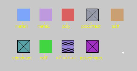
Here's a legend of relevant colors/layers:
Name
of layer
What the layer
represents
p or poly or polysilicon or
red
polysilicon (gate areas)
green or ndiff or ndiffusion
n-diffusion (n+ source/drain areas)
brown or pdiff or pdiffusion
p-diffusion (p+ source/drain areas)
blue or metal1 or m1
metal layer 1
purple or metal2 or m2
metal layer 2
pw or pwell
p-well
nw or nwell
n-well
nwc or nwcontact
metal1 to n-well contact (n-tub tie)
pwc or pwcontact
metal1 to p-well contact (p-tub tie)
ndc or ndcontact
metal1 to n-diffusion contact
pdc or pdcontact
metal1 to p-diffusion contact
polycontact
metal1 to poly contact
m2contact
metal2 to metal1 contact(via)
nfet or ntransistor
n-transistor
pfet or ptransistor
p-transistor
Some layers are created by crossing two layers. For example
drawing poly over ndiff (or vice versa) will produce an n-transistor. Contacts
are made by placing the box over the region of the contact and by painting the
appropriate contact. For example, to create a contact between ndiffusion and
metal1 layers, place a box over an overlap between the two layers and type
:paint ndc command.
For a complete list of layers use the Magic command :layers.
Basic
drawing
The box and cursor are used to select things on the layout window.
The left and right mouse buttons are used to position the box:
click on the left mouse button to position the lower left corner of
the box;
click on the right mouse button to set the upper right corner of the
box.
After drawing a box, you can paint layers
using command :paintlayer or by clicking the middle button as explained in the Cells, Paint and Layers section above. To select a
certain piece of the layout, move the cursor over the block you want to
select, and type s, which is a macro for
:select. A thin white outline is left around
the block to show it has been selected. Using the macro s repeatedly at the same spot will toggle through
electrically connected layers. This is a useful method to make a quick check
of how things are connected in your layout design. The macro S (macro for :select
more ) is just like s except that
it adds on to the selection, rather than replacing it. For a synopsis of all
the options to the :select command, type :selecthelp. You can also select an entire area of stuff.
Place the box over the area you want selected, and type :select area or macro
a. If you want to know what's selected, type
:what .
The following commands can be used to maneuver the selected part of the
layout:
:move (macro t), and macros q,
w, e, and r (to move by 1 lambda in
different directions); :stretch
(macro T), and macros Q, W, E, and R;
:upsidedown :sideways :clockwise :copy
(macro c) :delete (macro d) :erase
The best way to learn
these commands is to try them out. Often you may want to restore things after
you've made mistakes using:
:undo
(macro u) :redo (macro U)
Make sure that you delete any paint
that you don't want. Painting over something with another color just adds more
layers, your original paint will still be there underneath.
You can use the "." (dot) macro to repeat
the last command.
The easiest way to move around the graphics window is to use the "," (comma) macro, which centers the window around the
cursor position, together with the :zoomn
command, (or z and Z macros) to
zoom in and out.
In order to make your layout readable, and to prepare your layout for
extraction and simulation, you need to label it. First decide where you want
your label. Then left click and right click at that spot. You should end up
with a small cross (+). Then type
:label
labelname
Label names can be anything, but it
is
a good idea to use the labels that will correspond to circuit signals and
make
the layout readable. In particular, for digital simulation using the IRSIM
simulator (and some other applications that can use Magic outputs), it is
necessary to label the supply wires (nodes) as Vdd and GND
Note: Some layout editors will use the Vdd! and GND!
for power supply rails. The ! means that the node is global.
However, when using Magic and IRSIM together, the ! is not
recommended, because it prevents IRSIM from recognizing where you want to
have your supply voltage. Hence your circuit would operate without voltage
and not work, even though it passed gemini.
Wiring
Using the Box Tool to paint every little piece of a layout may not be the
most efficient. The Wiring Tool allows you to extend existing paint, and to
make contacts between layers. Once you have set down a few boxes of paint, you
can connect them together with "wires."
Switch to the Wiring Tool, typing either :tool or space-bar macro until you get there. Now
left click on the paint that you would like the wire to start from. Magic will
automatically select the width of the wire to be the largest box that can fit
in the paint you just clicked on. Then right click where you would like the
wire to end. The Wiring Tool only paints in horizontal and vertical lines. Try
to paint a couple of diagonals and see what happens.
Sometimes it's necessary to make a contact between different layers. When
different layers cross, they are insulated from each other. So you need to
explicitly tell Magic to make a contact between the layers. To do this, first
make sure that you are using the Wiring Tool (arrow cursor). Left click on one
layer where you want the contact to be made. Then middle click (i.e. press
both left and right button at the same time on a two-button mouse) on the
layer you want to connect to. The layers don't have to be overlapping to begin
with, but they must be immediately next to each other.
Design Rule Checking is an automatic feature of Magic. Magic knows certain
rules that your layout should satisfy so that the IC can be fabricated without
errors. In general, design rules specify how far apart various layers must be,
or how large various aspects of the layout must be for successful fabrication,
given the tolerances and other limitations of the fabrication process. As you
lay out the circuit, any time you place wires too close together, paint a
block too narrow, or make any other rule violations, Magic lets you know
immediately by splattering small white dots around the area of concern. Once
the error has been corrected the dots will disappear. For example, paint a
pair of metal1 wires fairly far apart, select one, and move it closer to the
other. The white dots will appear once the wires are less than 3 lambda apart.
In general, you can find out what design rule is violated by clicking the
cursor on the white-dots area and by typing :drc
why or macro y.
The built-in Magic extractor computes from the layout
the information needed to run simulation tools such as Spice or IRSIM. The
information includes the sizes and shapes of transistors, and the
connectivity, resistance, and parasitic capacitances of nodes. Both
capacitance to substrate and several kind of internodal coupling capacitances
are extracted. Magic's extractor is both incremental and hierarchical: only
part of entire layout must be re-extracted after each change, and the
structure of the extracted circuit parallels the structure of the layout being
extracted.
The command
:extract
produces a separate .ext file for each .mag
file in a hierarchical design. If your Magic layout is just a single cell
named cell-name.mag, the extraction output will be placed in the file
cell-name.ext.
If your layout includes subcells, to extract all the
edited subcells, use the command:
:extract all
or to extract just the selected (current) cell type
:extract
cell-name
The output will be
placed in the file cell-name.ext.
Extraction is explained in more detail in the Magic Tutorial #8: Circuit Extraction. The output .ext file is
used to generate the netlist file suitable for simulation. Spice simulation
based on the file extracted from layout is explained in the Spice
page.
A
Step-by-Step Example: Layout of a CMOS Inverter
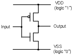
Here is a step by step example of how to layout a CMOS logic inverter shown
below:
The inverter consists of an NMOS transistor M1 and a PMOS transistor M2.
The channel width W and the channel length L of the two devices will
be set at 3.0um and 6.0um, respectively. The sizings of
of each transistor allow designers to custom the current-drive for
each gate based on fan-in, fan-out, and other influential factors.
Note that the source and the body (p-
substrate) of the NMOS are connected to ground (GND node), while the source
and the body (n-well) of the PMOS are connected to the positive supply (Vdd
node) even though they are not shown. This is because for most
introductory circuit classes, the three port model is used (shown),
however,
when we are dealing with VLSI design, we must utilize the four-port model
which accounts for substrate connections which are vital to preventing
the body-effect.
We assume that the target fabrication technology is AMI C5N 0.5u CMOS
process. The technology name is scn3me_subm. The unit length lambda for
this technology is lambda=0.3um. Therefore, the width for both the NMOS
and PMOS transistors in lambda is 10 lambda and 20 lambda, respectively
(e.g. 3.0um/0.3um/lambda = 10 lambda).
In this example, we use basic Magic drawing command to layout the
inverter.
Remember that you can undo just about everything by typing :undo or u.
Start Magic from the Unix prompt:
prompt> magic
inverter
Expand the graphics window over the screen, but so that
you can still see the text window prompt. Remember that the graphics window
must be active and the cursor must always point to the graphics window. Zoom
out and show the lambda grid so that it is easier to see what you are doing.
:zoom 0.5 :grid 1
The order in which layers are
placed in the graphics window is not important, and so the layout steps
described here are by no means unique. Since the device channel width W and
length L are specified, we can start by painting the device active areas:
p-diffusion for PMOS and n-diffusion for NMOS.
The PMOS transistor has the channel width W=6.0um, which is equal to 20
lambda in the selected technology. The channel length L=0.6um equals 2 lambda.
The design rules specify that we need at least 4 lambda for the source and
drain contacts, plus at least one lambda between the poly gate and the
source/drain contacts. Using left and right mouse click, make a box 20 lambda
high and 2+4+4+1+1=12 lambda wide. The command:
:paint pdiff
paints
the PMOS active area (p-diffusion). The NMOS transistor has the channel width
W=3.0um, which is equal to 10 lambda, and the channel length L=0.6um (2
lambda). Make a 10 lambda (height) by 12 lambda (width) box under the
p-diffusion area you already painted. You may want to align the left edge of
the box with the left edge of the p-diffusion area. The command:
:paint ndiff
paints the NMOS active area (n-diffusion). A design rule is
that
n-diffusion must be at least 12 lambda away from p-diffusion. If you placed
the n-diffusion area closer to the p-diffusion area, white dots will appear
indicating design rule violation. To move the n-diffusion area, point to the
area, type macro s to select the area, and use macros q, w, e, or r to move the area until the
white dots disappear. At this point, your layout should look something like
this:
Next, paint horizontal, 6-lambda metal1 wires that will serve as Vdd and
GND. Although design rules allow for minimal widths of 4 lambda for m1,
making power and ground "rails" wider helps current flow since these wires
are used extensively and are connected in many places.
Align the top edge of the Vdd wire with the top edge of the p-diffusion.
Make this box about 25 lambda wide. The command:
:paint metal1
paints
the metal1 (Vdd) wire. Then, select the Vdd wire using the s macro, position the cursor to
the lower left corner aligned with the left edge of the Vdd wire and the
bottom edge of the n-diffusion area, and type c. This will copy the metal1 wire
to where the GND wire should be.
To make a contact between the Vdd wire and p-diffusion
(source of the PMOS), make a box over at the overlap between the metal1 and
pdiffusion areas and type the command:
:paint pdc
To make a
contact between the GND wire and n-diffusion (source of the NMOS), make a box
over the overlap between metal1 and n-diffusion layers. Note that design rules
specify that the minimum contact area is 4 lambda by 4 lambda. Type the
command:
:paint ndc
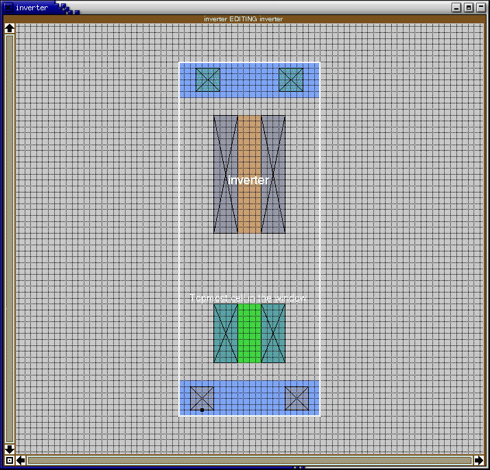
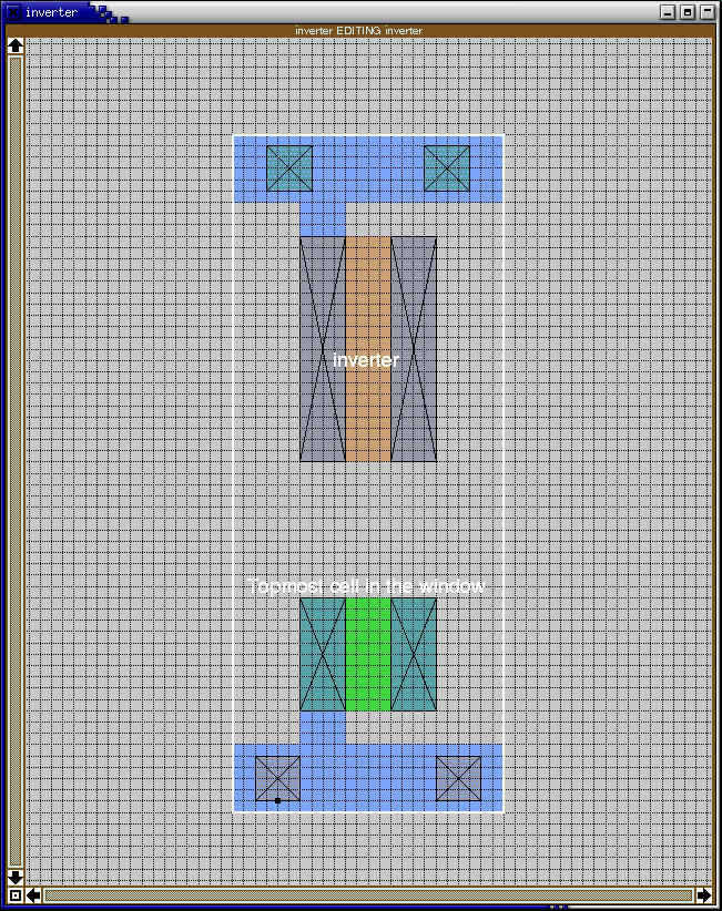
At this point, your layout should look like this:
The next step is to paint the n-well area where the
PMOS is located. Actually, this step is not necessary, because Magic knows
that the n-well is needed for the specified technology, and would
automatically generate the required layer for fabrication. Nevertheless, it is
a good practice to place the n-well layer by hand. Place a box extending at
least 5 lambda above and below the p-diffusion, and as wide as the metal1
wires. The command:
:paint nwell
paints the n-well for the PMOS. At this point, we can also add
contacts between the GND wire and the p-substrate (body of the NMOS), as well
as between the Vdd wire and the n-well (body of the PMOS). Place a 4 lambda by
4 lambda box over the metal1 wire, but do not overlap the PMOS source contact
you already made. The command:
:paint nwc
paints the n-well to metal1 contact. If the contact is too close
to the pdiff to metal1 contact, white dots will appear. Select the
n-well-to-metal1 contact you just created and use Q or R macros to move it away until
the white dots disappear. Repeat the same to create a metal1 (GND) to
p-substrate contact. Type:
:paint pwc
The layout should look like this:
The body contacts (such as the ones you just created)
should always be located as close as possible to the device source contacts to
minimize the possibility of latch-up that plagues CMOS circuits. It is also a
good practice to put as many body contacts as possible.
The next step is to make drain contacts, connect the
drains of the NMOS and the PMOS, and lay out the output node using metal1. The
steps are the same as the steps you used to create the Vdd and GND wires and
the source contacts. Note that the simplest way to paint a box is to simply
click the middle button (i.e. both the left and the right mouse button on a
two-button mouse) over the area already painted with the desired layer.
You should now have a layout that looks approximately
like this:
The next step is to paint and connect the gates of the
NMOS and the PMOS. Position a 2-lambda wide horizontal box to overlap the
middle n-diffusion area by at least 2 lambda on both sides. Type
:paint poly
Notice how the area of poly-to-ndiffusion overlap
changes to green/red stripes. This is the channel of the NMOS. Do a similar
poly box over the p-diffusion. Correct the size or position of the poly areas
if you have white dots indicating design rule violations. Connect the poly
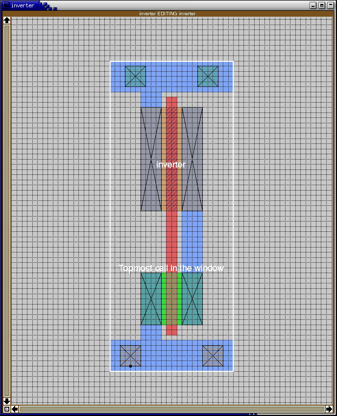
areas and make the input node. The layout should look like this:
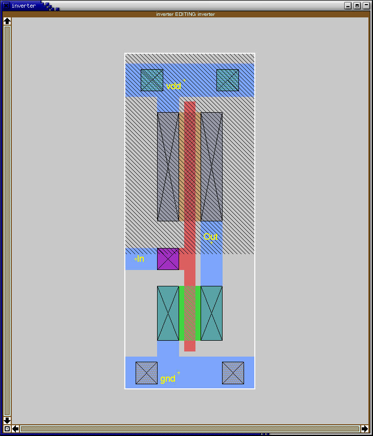
The final step is to put labels on the important
signal
nodes. Left click and than right click on the poly, close to the left edge.
You should see a small yellow + at that spot. Then type:
:label in
to label the poly as the input node of the inverter.
Similarly, label the Vdd wire as Vdd, the GND wire as GND, and the output
wire as out. The final layout should look like this:
The grid has been turned off using the
g macro, and the circuit
diagram
is shown again for easy comparison with the layout.
Save the layout you created:.
:save
Extract the layout to create the output file that will be used with a
simulator:
:extract
To exit Magic,
type:
:quit
Cell
Hierarchies
The concept of cells is essential for efficient and structured layout of
VLSI circuits. The basic idea is quite simple: if you created a layout for a
building block (such as an inverter) that can be used in another design or
is
going to be used many times in the current design, then it is useful to
simply
include this layout of the building block as a cell. Every time you
create and save a circuit in Magic, you have effectively created a
cell. Each cell can be included in the hierarchy of a new
circuit. The
cells you created or the cells created by others in a library can then be
put
and connected together in a new circuit. Here are basic commands related to
working with cells.
Start a new circuit. Then,
:getcellname --
includes a cell that you want in the new circuit.
The included
cells are shown as "black boxes" with only the instance names showing. No
details of the included cell are shown. This is known as the unexpanded
form.
You can select and manipulate each cell as you could a box of paint. In
order to "connect" cells together, you need to know where the "connection
points" of a cell are. Thus, expand the cell and paint wires between
appropriate points of the cells. The following macros are used to expand or
unexpand cells:
x – expands a selected
cell,
all details are visible. X –
unexpands
a selected cell, all details are hidden.
If you included a
number
of pre-designed identical cells and you realize that you need to make one
small change to all of them, you can edit just one cell by itself and the
changes will be reflected in all the other cells. To edit the cell, type:
:load
cell-name
Magic will load that cell (and all of
its sub-cells) into the window. Once all changes have been made, :save your changes and
:load the circuit you were working on. All changes will be
reflected in your circuit's cells.
A more detailed explanation of the cell hierarchies can be found in the Magic Tutorial #4: Cell Heirarchies.
Magic
Tutorials, Summary of Commands, and Complete Manual Pages
Magic comes with a set of tutorials that go through commands, macros, and
mouse functions. You may want to go first through the tutorials labeled with
*. Please do not print the
tutorials or the manual pages on the lab printers - these are large files that
can best utilized on-line.